Is A Sheet Of Copper Ohmi

No Freaking Way This Is Brilliant Why Didn T I Ever Think Of That Duh Jewelry Making Tools Jewelry Making Tutorials Creating Jewelry

The Late Hauterivian Faraoni Oceanic Anoxic Event At Rio Argos Southern Spain An Assessment On The Level Of Oxygen Depletion Sciencedirect
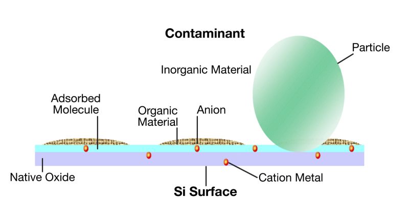
Wafer Surface Cleaning

Materials Free Full Text Luminescence In Sulfides A Rich History And A Bright Future Html
Nanomaterials Free Full Text Supercapacitor Performance Of Nickel Cobalt Sulfide Nanotubes Decorated Using Ni Co Layered Double Hydroxide Nanosheets Grown In Situ On Ni Foam Html
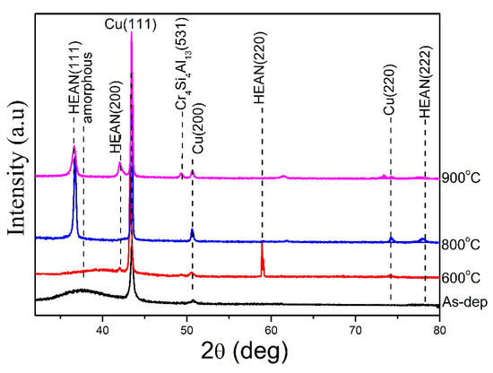
One of the major challenges in the miniaturization of modern microelectronic devices is the development of future diffusion barrier materials against the diffusion of cu.
Is a sheet of copper ohmi.

Valentino Pearly Lace Frame Sunglasses Black Multi 346 Via Polyvore Sunglass Frames Sunglasses Valentino Sunglasses
Https Iopscience Iop Org Article 10 1149 2 0101901jes Pdf

Metal Assisted Chemical Etching Of Silicon A Review Huang 2011 Advanced Materials Wiley Online Library

Detrital Garnet And Chromian Spinel Chemistry Of Permian Clastics In The Renge Area Central Japan Implications For The Paleogeography Of The East Asian Continental Margin Sciencedirect

Japanese Art Mountain Fuji And Sakura Cherry Tree Blossoms Etsy Japanese Woodblock Printing Japanese Art Woodblock Print

Inspired By Harry Potter Gryffindor Charm By Onaspelledwind 37 00 With Images Harry Potter Outfits Harry Potter Jewelry Harry Potter Accessories
Experimental Investigation Of The Photocapacitance Effect In Organic Heterojunction Devices Springerlink
Avs Scitation
Entropy Free Full Text Diffusion Barrier Performance Of Alcrtatizr Alcrtatizr N High Entropy Alloy Films For Cu Si Connect System Html

Influence Of Tantalum S Crystal Phase Growth On The Microstructural Electrical And Mechanical Properties Of Sputter Deposited Tantalum Thin Film Layer Sciencedirect
Graphene Si Schottky Solar Cells A Review Of Recent Advances And Prospects Rsc Advances Rsc Publishing Doi 10 1039 C8ra08035f
Https Arxiv Org Pdf Cond Mat 0312540

Fluorine Compounds Inorganic Hydrogen Smith Major Reference Works Wiley Online Library
Https Avs Scitation Org Doi Pdf 10 1116 1 5080445

Influence Of Ti3ni4 Precipitates On The Indentation Induced Two Way Shape Memory Effect In Nickel Titanium Sciencedirect
Http Www Tandfonline Com Doi Pdf 10 1080 714037708
Http Accelconf Web Cern Ch Icap2015 Papers Proceed Pdf

A Review On Mechanical Joining Of Aluminium And High Strength Steel Sheets By Plastic Deformation Sciencedirect
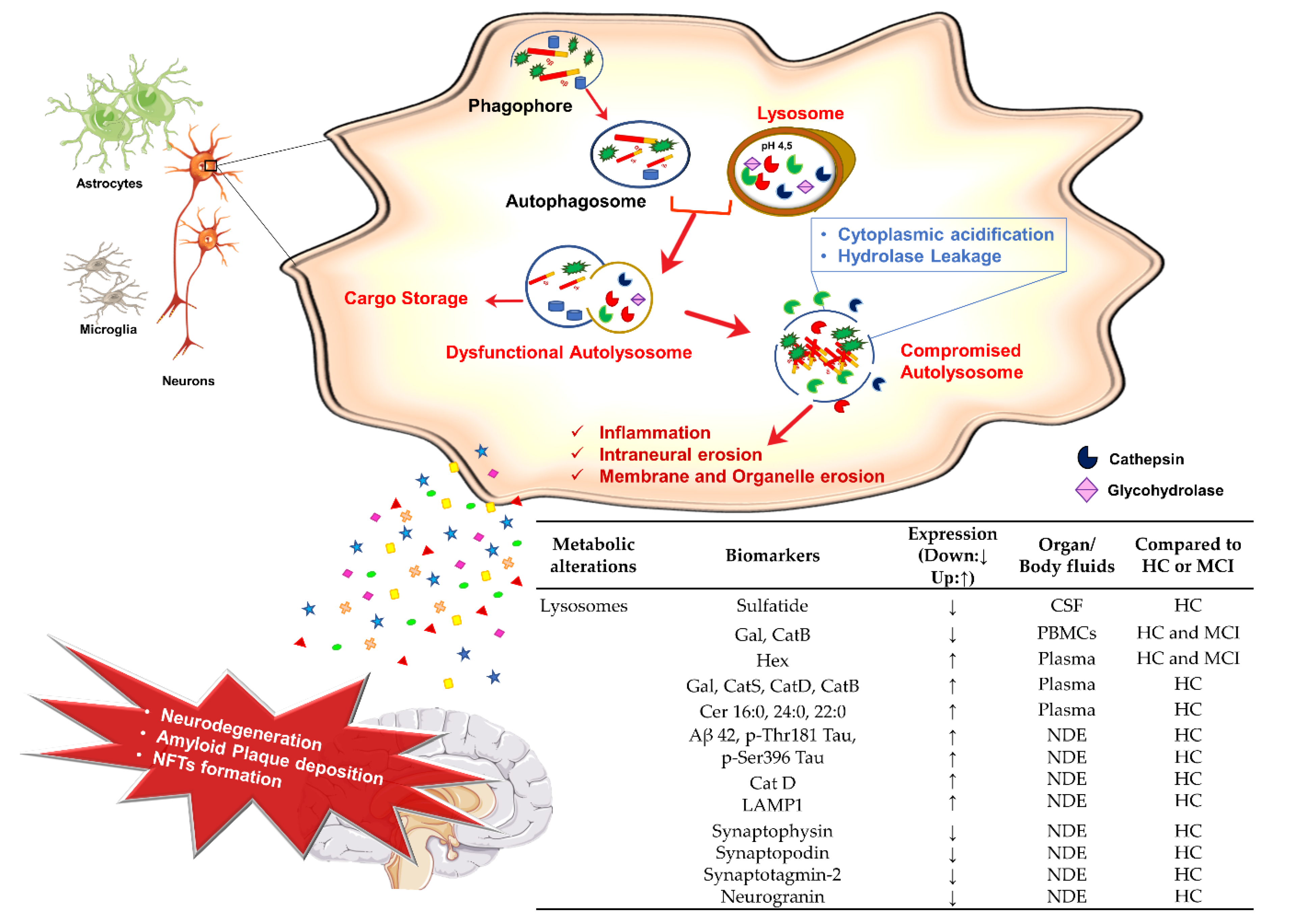
Jpm Free Full Text The Other Side Of Alzheimer S Disease Influence Of Metabolic Disorder Features For Novel Diagnostic Biomarkers Html
Page 3 Iill High Resolution Stock Photography And Images Alamy
Https Ieeexplore Ieee Org Iel7 8868012 8878909 08879146 Pdf
Https Onlinelibrary Wiley Com Doi Pdf 10 1002 Pip 3141
Https Greet Es Anl Gov Files Light Duty Vehicle 2016

High Rate Sio2 Deposition By Oxygen Cold Arc Plasma Jet At Atmospheric Pressure Han 2008 Plasma Processes And Polymers Wiley Online Library
Https Www Worldscientific Com Doi Pdfplus 10 1142 S0218625x01001221
Https Pubs Rsc Org En Content Articlepdf 2019 Ra C8ra08035f

Abnormal Sds Page Migration Of Cytosolic Proteins Can Identify Domains And Mechanisms That Control Surfactant Binding Shi 2012 Protein Science Wiley Online Library
Https Www Sciencedirect Com Science Article Pii 092023079290011o Pdf Md5 24c7247483ef1f376e1f8e70c80ed767 Pid 1 S2 0 092023079290011o Main Pdf
Http Www Iaea Org Inis Collection Nclcollectionstore Public 26 034 26034122 Pdf
Http Pubs Acs Org Doi Pdf 10 1021 Acsami 7b09149 Src Recsys
Https Www Sciencedirect Com Science Article Pii S0026057600813896 Pdf Md5 Ec0223f5045ca82cb886d68eb52fdb0f Isdtmredir Y Pid 1 S2 0 S0026057600813896 Main Pdf
Https Files Eric Ed Gov Fulltext Ed219646 Pdf

Pdf Hot Stamping Of Ultra High Strength Steel Parts
Https Www Jstor Org Stable 40267983

Womens Hairdressing Utamaro Yuyudo Ukiyo E Art Poster Zazzle Com Japanese Art Prints Japanese Woodblock Printing Japanese Prints

Fundamentals And Applications Of Plasma Cleaning Sciencedirect

Us10541173b2 Selective Deposition Method To Form Air Gaps Google Patents
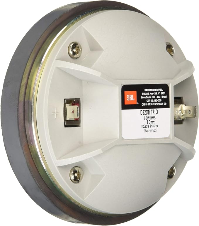
Amazon Com Selenium D220ti 1 Inch 8 Ohm Titanium Horn Driver
Http Ciqm Harvard Edu Uploads 2 3 3 4 23349210 Songy2015 Pdf
Https Apps Dtic Mil Sti Pdfs Ada383173 Pdf

Static Elimination In Vacuum Using Plasma Jet Sciencedirect
Https Digitalcommons Unl Edu Cgi Viewcontent Cgi Article 1210 Context Animalscidiss
Https Onlinelibrary Wiley Com Doi Pdf 10 1002 3527602534
Https Web Wpi Edu Pubs E Project Available E Project 101111 173945 Unrestricted Comm Nav Antenna Mqp Pdf
Source : pinterest.com
